Working with development boards and programmers tends to be quite annoying. Every module and MCU and converter board is a bundle of wires connected to multiple other wires that all slide around the desk, can get lost, can get tripped on, and it can be easy to forget the pinout of a particular board and converter. After dealing with these issues myself and seeing many fellow engineers go through the same, I decided to make it easier for me and build a single integrated box that contains converters for the protocols I use the most often with their associated circuitry, pinouts clearly labeled, and firmware loaded already.
This project prominently features the three following projects/chips:
- The official Raspberry Pi Pico Probe firmware running on the Raspberry Pi Pico
- The dirtyJTAG firmware running on STM32 Blue Pill (clone, in this case)
- CH340 USB-to-UART converter
The project first started with looking into my requirements. I needed:
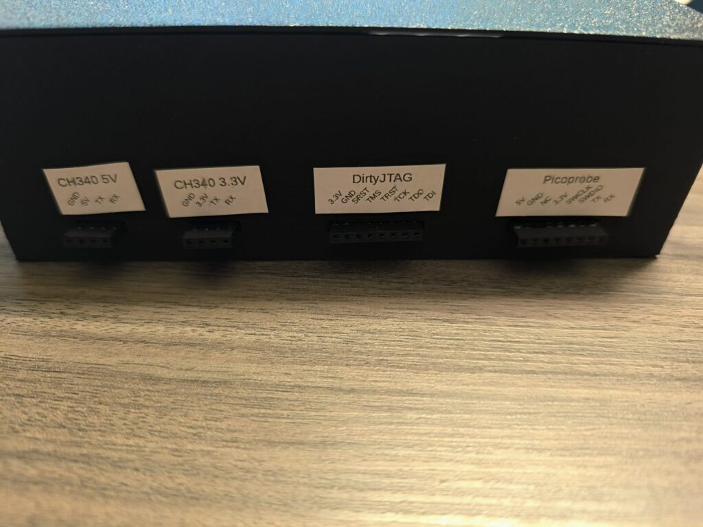
- SWD
- JTAG
- 2x 3.3V UART
- 5.0V UART
I visualized my primary use case as programming/debugging 3.3V microcontrollers (which I do very often) and potentially programming and debugging 3.3V FPGAs. I also wanted to have 5V UART for when I’m working on older microcontrollers or even microprocessors.
Initially, I wanted to use the same UART with level shifters to select between 3.3V and 5V. However, this turned out slightly more difficult due to the fact that the TXB0108 I had planned to use was badly suited for my use case. The TXB0108 has a high output impedance, meaning that over long cables (such as debugging probe cables) with a higher inductance, the slew rate will be much lower, thus severely limiting the maximum data rate. Additionally, this would require some kind of circuit to switch the voltage, and this was extra work that I wouldn’t have to do if I just put two UARTs. Thus, I put two UARTs.
For the UARTs, I chose the common and convenient CH340N USB-to-UART converter. The -N suffix is particularly important here because it’s a small 8-pin package that is easy to configure – only two extra capacitors needed. The chip’s power supplies work the following way – there’s a “VCC” and “V3” pin. VCC is the logic voltage. It determines the voltage level of the CMOS signals coming out of the CH340, such as TX, RX, and any of the other signals on the other packages (such as RTS). V3 is the voltage for the USB subsystem and it is generated inside of the CH340 from the VCC pin. Thus, you don’t need to connect V3 to anything except to a 100nF decoupling capacitor. VCC needs to be decoupled with 100nF too, as well as with a 10uF decoupling capacitor.
For both SWD and JTAG, I wanted to use projects I have used before and know are reliable. I also wanted to avoid buying specialized hardware and just use development boards I have available to me. For this reason, for SWD, I chose to use the Raspberry Pi Pico Picoprobe, an official firmware by Raspberry Pi that turns a Raspberry Pi Pico into an SWD+UART debug probe. This fulfilled both an SWD requirement and a UART requirement. I used the following tutorial to install the firmware and connect the signals: https://mcuoneclipse.com/2022/09/17/picoprobe-using-the-raspberry-pi-pico-as-debug-probe/
For JTAG, I chose dirtyJTAG with an STM32 Blue Pill clone board. I only chose this specific configuration because it’s very cheap and the most tested variant of this firmware. I used the following tutorial for the firmware: https://github.com/dirtyjtag/DirtyJTAG/blob/master/docs/install-bluepill.md
If you’re building this yourself, I recommend using a second Raspberry Pi Pico with this firmware, because it gives you an additional 3.3V UART: https://github.com/phdussud/pico-dirtyJtag
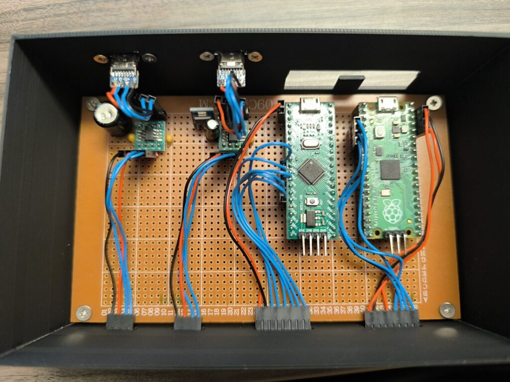
For the physical construction, I wanted a 3D-printed casing containing a generic 9x15cm protoboard that you can find online for very cheap. I soldered the components on the protoboard and then ran connectors to cutouts in my casing design. The casing was just designed with four screw holes and the size to accommodate the 9x15cm protoboard with a bit of margin on the sides to allow for a thin screwdriver to screw in the screws. The casing had space for the USB ports on one side and the connectors on the other. The connections go as follows: dev board/CH340 -> male header -> cable -> female header on case. I did it like this because I wanted to have the option of lifting up the cover and connecting wires directly to the male headers, or if I want to have a more convenient experience, to use the female headers.
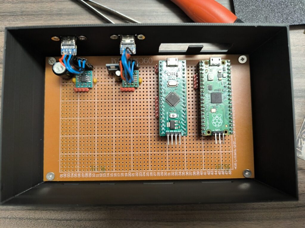
After designing and printing the case, I assembled each part. Initially I designed the case to permanently solder in the dev boards, so with the 20-pin female headers, it was actually too tall and needed modification. The final STL takes this into account.
I also added some labels so that I never need to look up the pinout, and voila!
BOM
- 4x 20 female 2.54mm header pins (optional, for mounting the dev boards)
- 2x 4 female 2.54mm header pins
- 4x 4 male 2.54mm header pins
- 1x 2 male 2.54mm header pins
- 1x 6 male 2.54mm header pins
- 2x CH340N (other variants work but are less convenient)
- 2x SOIC8-to-DIP8 adapter boards
- 2x 10uF electrolytic capacitor (>10V minimum)
- 3x 100nF ceramic capacitor
- 1x AMS1117 module or similar 5V to 3.3V regulator
- 2x USB-C breakout module (or whatever USB you prefer)
- 1x 9x15cm universal protoboard
- 1x Raspberry Pi Pico
- 1x STM32 Blue Pill (note: using only 2x Pico or 2x Blue Pill is also an option)
For the custom wires (note that all DuPont-style connectors and their respective header pins can be replaced with similar JST connectors or any other 2.5/2.54mm connector style):
- Approximately 2 meters of 24-26AWG copper wire (I used red for power, black for ground, blue for data)
- 6x 4-pin DuPont housing
- 8x 1-pin DuPont housing
- 1x 2-pin DuPont housing
- 1x 6-pin DuPont housing
- 2x 8-pin DuPont housing
- 8x male DuPont pins
- 46x female DuPont pins
- For the PLA housing:
- Approximately 90g of PLA filament
- 4x M3 4mm-long screws