This February I participated in this year’s Vex Robotics Challenge (VRC) with a team from my school. We won an award for our design of the robot, and it was truly a good design.
I programmed the robot so I got to learn its capabilities, and when looking at the robot controller (Vex V5 Brain) I was amazed. It features (according to the company’s webpage): -Two Cortex A9 at 667 MHz -Two Cortex M0 at 32 MHz each -One FPGA I decided to research it further and I found an amazing forum thread on the official website which had photos of the Brain and an outline of its major components. So, I decided to analyze it in this blog post and propose an alternative system in the end.
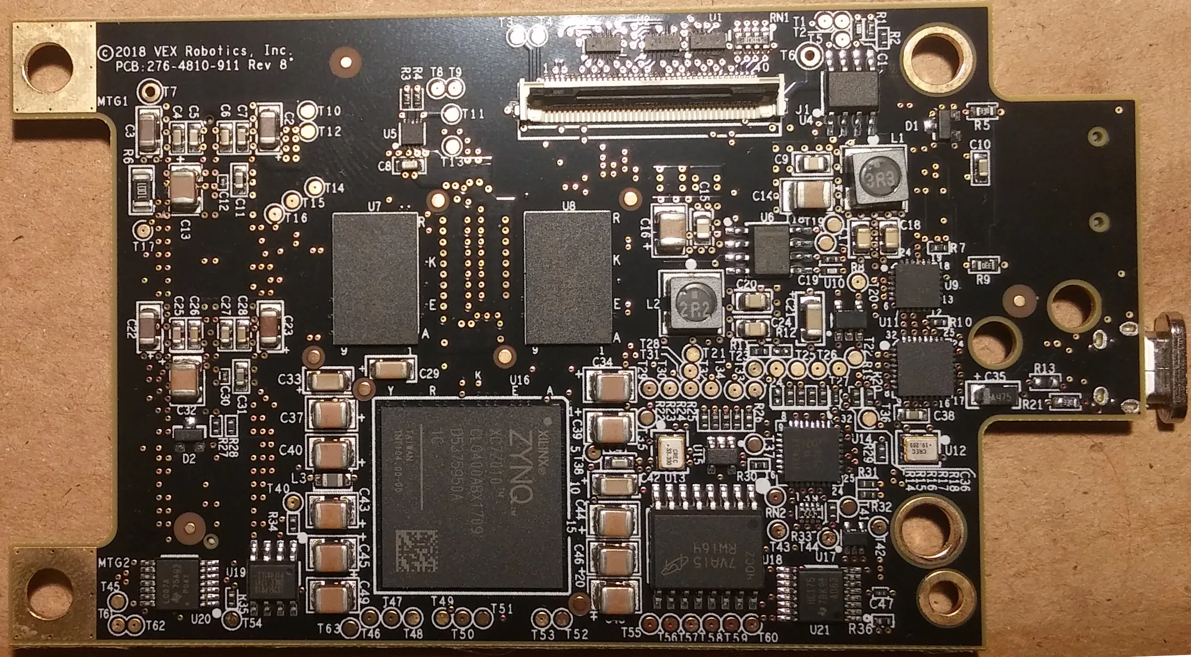
This impressive hardware comes with an impressive cost – 349.99$. The dual Cortex A9 + FPGA combination immediately made me think that they’re using a (AMD) Xilinx Zynq SoC, and indeed they are – specifically, an XC7Z010. Both the photos and the specs for the robot brain support this. At a current price (post-COVID FPGA prices have increased the most out of any chip) of 74.83$, this is a hefty chip and is definitely the brain of the Brain. One number to keep in mind is 1333 MIPS for the main processor (for a single core) taken from their marketing page (or 2666 both cores).

The other processor is an NXP824J, which is a member of the LPC82X family, and since it’s in a QFN package, is definitely a LPC824M201JHI33 (I found that from the datasheet) with a unit cost of 3.38$ in single quantity, but below 2$ after 500 pieces. It’s important to note that the brain has one NXP824J, while each component has one as well. This dramatically increases the microcontroller count – if all 21 smart ports are connected, that’s a total of 22 microcontrollers + a Zynq. This processing power is incredible, but what is it used for?
One thing that really made me like the Vex V5 ecosystem was the extensive monitoring. All major parameters of the components used – motors, WiFi, controllers – have their associated data and get graphed on the hardware and display of the Brain itself. Even though most of the components require tiny bandwidth, some like the vision sensor have a larger bandwidth requirement (will be discussed later), and the provided monitoring in real time is pretty unique.
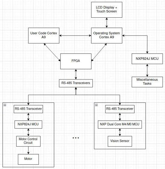
However, while looking at the hardware, one question always came to me: is this processing power seriously needed? The Vex V5 hardware doesn’t do AI, neither does it do any complex GUI and neither would you want any complex GUI on a robot whose display is buried under mountains of parts. The number of programs you can store is not significantly increased, and neither is the 128MB of RAM able to be used for anything. In particular, why use an FPGA?! For the FPGA, there is a massive number of extremely complex power management components needed. Our battery during the competition drained extremely fast even when the robot was doing nothing, and the Zynq’s datasheet states the quite large quiescent current consumption. Looking at the processor board, most of it’s filled up with power management ICs (PMICs) for the FPGA. All the high-quality power handling needed raises the system cost dramatically, as well as the cost. I drew an approximate system diagram for how the components interact with each other based on my observations and intuition.
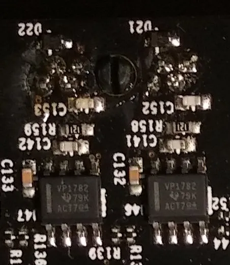
One clue, for the FPGA at least, came from the board design itself. All smart ports are connected with an SN65HVD1781 RS-485 driver on both sides. Given that this is a design with motors and similar high-current components, using robust communication such as RS-485 somewhat makes sense. However, again, with all 21 smart ports, that’s 42 RS-485 drivers, and they go for >3$ even in quantity. As RS-485 is usually used with UART in the communication layer, a microcontroller can’t pull off the task of handling 21 UARTS simultaneously. The most UARTs I’ve seen on a microcontroller is 8, on the very impressive RISC-V CH32V307 (3.5$ in single quantity, 3-2.4$ in 100+ quantity, depending on the package). This made me think – can I design a better system?
In my opinion, the main issue with the system above is the CPU -> FPGA -> RS-485 transceiver -> RS-485 transceiver -> microcontroller -> ASIC/circuit -> component pipeline. In a general embedded system, often the main microcontroller directly controls the component, or does it through a slave microcontroller/ASIC. The way it’s done here adds to the cost and complexity significantly, and in my opinion there is a simpler alternative.
RS-485 is usually used due to its good handling of noise in industrial environments over long distances. Here, however, all of the cabling is below half a meter, so that’s somewhat unneeded, even though the environment is noisy. There is, though, another standard made specifically for this purpose – CAN. Made for vehicles with hundreds of microcontrollers inside, CAN handles all of the complex communication and collision detection in hardware, as well as offering the capability for a single bus to communicate with all devices. CAN requires a transceiver, however because one bus is used (unlike the separate 21 buses for RS-485/UART in the Brain), only one transceiver on the Brain side would be necessary. A CAN transceiver is around 0.5$, even from reputable manufacturers (TI/NXP/Microchip). Using CAN bus would allow a single MCU with a single CAN transceiver to communicate with all connected components to the brain.
The data rate of CAN is around 1Mbps, however I don’t think this would be an issue at all. Even the most complex peripheral, the vision sensor, only takes a picture every 20ms and does the processing on-board. Only the bounding box results are sent to the brain – a couple of bytes per transfer at most. It’s also unlikely that it will be running at its max speed in general. The motors also only report a few bytes of data per second. No sensor, no motor, no peripheral would really exceed the CAN bus max speed, especially since all components do the bulk of their processing on-board.
Thus, the Zynq is quite unnecessary and I propose replacing it with the aforementioned CH32V307. One V307 for the user code, one for the operating system (an RTOS) and one for handling the peripherals/CAN would work perfectly and cost <10$ in total. This would also remove the power handling circuitry, which means that around 100$ of cost can be reduced. The RISC-V QingKe V4F core used inside has no official MIPS/MHz number, but since it’s supposed to be a drop-in replacement for an ARM Cortex M4F, taking the 1.25MIPS/MHz number gives 540 MIPS. QingKe V4F is based on RV32IMAFC, which according to some sources is actually much faster, but even 540 MIPS is way more than enough for the task. Even 54, and probably even 5.4 MIPS could be enough for handling all the robot’s tasks. A Motorola 68000 was approximately that fast, and it’s still used for industrial robots! V307s use a single 3.3V input, support 128MB of external RAM (if needed), use much less power, and integrate practically all of the features the Brain needs. Even if one doesn’t want to use a Chinese RISC-V, equivalent STM MCUs for approximately double the price (STM32F446) accomplish the same task and are slightly faster.
On the other hand, each component still has to use a CAN transceiver, however the MCU choice can also be changed here to the very fast and very cheap CH32V203. At 0.5$ per MCU, it’s full of integrated peripherals which can do all the tasks of motor control and sensor reading, while still having hardware CAN and being significantly faster than the NXP824J used.
In total, the system cost in most areas can be reduced by a factor of 2-10, given the reduced power handling and complexity, while practically all of the features would remain identical. The CH32V307 can easily render a GUI of the complexity needed, while handling interrupts and doing processing. Three of them? No processing task is too hefty. Given the advanced floating point routines, even AI isn’t out of the question. If it is, a Sipeed M1s for 7$ can add advanced AI, WiFi, Bluetooth, as well as a RISC-V application processor and an MCU which together can replace two CH32V307s. With 768KB SRAM and 64MB SRAM, as well as a 64-bit application processor at 480MHz, its capabilites would probably exceed the original system’s.
If the FPGA is a hard requirement, the proposed system can be augmented with a simple Lattice FPGA for 5$, and even if the 28K logic blocks are essential, that’s less than 20$ in FPGA. A nice display with a similar size and better resolution like the Brain’s can be bought from Buydisplay.com for ~12$. Or, since we have the budget, why not a 7 inch display for 30$?
The goal of this blog post wasn’t to complain about the Vex V5 Brain, rather I aimed to have it as a discussion about new technologies which make such older designs, in my opinion, unnecessarily expensive and unavailable for beginners. The quality of Vex is undeniable, and I will even ardently claim that the 350$ for the V5 Brain is a perfectly good price with the hardware given. However, changing it to simpler hardware would have significantly reduced the cost while retaining all of the capabilities. A rough calculation given the prices above would give 10.5$ for the MCUs (V307 + M1s/2 V307s), 3$ at most for the power management, 0.5$ for the CAN transceiver, 12$ for the display, approximately 15$ for miscellaneous components (connectors, other passives), and approximately 10$ for the enclosure. At 50$ in components (whose price dramatically reduces in quantity), all the rest of the money can go to reducing the price or developing software and support. I know that much of the 350$ in the Brain goes towards software development, however I doubt that much of the Zynq is being used, and if it is, then it’s not being used efficiently. Simply said, this can’t really be done better, but it can be done cheaper and simpler while all the capabilities remain the same.
Maybe I should be the one to make this work…